CUHK
News Centre
CUHK Faculty of Engineering Presents a Game-changing Nanoscale 3D Printing Technology – Femtosecond Projection Two-photon Lithography Boosts Printing Speed by up to 10,000 Times
Ultraprecise 3D printing technology is a key enabler for manufacturing precision biomedical and photonic devices. However, the existing printing technology is limited by its low efficiency and high cost. Professor Shih-Chi Chen and his team from the Department of Mechanical and Automation Engineering, The Chinese University of Hong Kong (CUHK), collaborated with the Lawrence Livermore National Laboratory to develop the “Femtosecond Projection Two-photon Lithography (FP-TPL)” printing technology. By controlling the laser spectrum via temporal focusing, the laser 3D printing process is performed in a parallel layer-by-layer fashion instead of point-by-point writing. This new technique substantially increases the printing speed by 1,000 – 10,000 times, and reduces the cost by 98%. The achievement has recently been published in Science, affirming its technological breakthrough that leads nanoscale 3D printing into a new era.
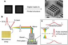
The conventional nanoscale 3D printing technology, i.e., two-photon polymerisation (TPP), operates in a point-by-point scanning fashion. As such, even a centimeter-sized object can take several days to weeks to fabricate (build rate ~ 0.1 mm3/hour). The process is time-consuming and expensive, which prevents practical and industrial applications. To increase speed, the resolution of the finished product is often sacrificed. Professor Chen and his team have overcome the challenging problem by exploiting the concept of temporal focusing, where a programmable femtosecond light sheet is formed at the focal plane for parallel nano-writing; this is equivalent to simultaneously projecting millions of laser foci at the focal plane, replacing the traditional method of focusing and scanning laser at one point only. In other words, the FP-TPL technology can fabricate a whole plane within the time that the point-scanning system fabricates a point.
What makes FP-TPL a disruptive technology is that it not only greatly improves the speed (approximately 10 – 100 mm3/hour), but also improves the resolution (~140 nm / 175 nm in the lateral and axial directions) and reduces the cost (US$1.5/mm3). Professor Chen pointed out that typical hardware in a TPP system includes a femtosecond laser source and light scanning devices, e.g., digital micromirror device (DMD). Since the main cost of the TPP system is the laser source with a typical lifetime of ~20,000 hours, reducing the fabrication time from days to minutes can greatly extend the laser lifetime and indirectly reduce the average printing cost from US$88/mm3 to US$1.5/mm3 – a 98% reduction.
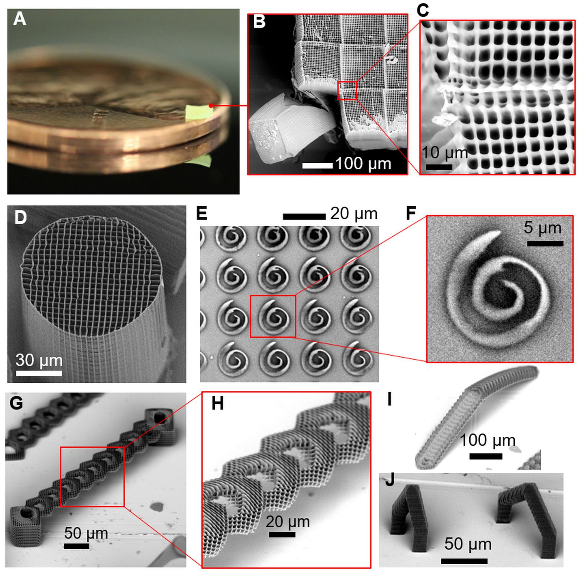
Due to the slow point-scanning process and lack of capability to print support structures, conventional TPP systems cannot fabricate large complex and overhanging structures. The FP-TPL technology has overcome this limitation by its high-printing speed, i.e., partially polymerised parts are rapidly joined before they can drift away in the liquid resin, which allows the fabrication of large-scale complex and overhanging structures, as shown in Figure 1 (G). Professor Chen said that the FP-TPL technology can benefit many fields; for example, nanotechnology, advanced functional materials, micro-robotics, and medical and drug delivery devices. Because of its significantly increased speed and reduced costs, the FP-TPL technology has the potential to be commercialised and widely adopted in various fields in the future, fabricating meso- to large-scale devices.
The research team has been supported by the Innovation and Technology Commission (ITC), receiving multiple Innovation and Technology Fund (ITF). The project also received support from the Lawrence Livermore National Laboratory, under the Department of Energy of the United States. The research team has received multiple U.S. patents related to this project and the results were published in Science in October. Science is regarded as one of the most prestigious academic journals in the world, published by the American Association for the Advancement of Science (AAAS).
Fig. 1. Printing of complex 3D structures with submicron resolution via FP-TPL. (A to C) Millimeter-scale structure with submicrometer features supported on a U.S. penny on top of a reflective surface. The 2.20 mm × 2.20 mm × 0.25 mm cuboid was printed in 8 min 20s, demonstrating a 3D printing rate of 8.7 mm3/hour. In contrast, point-scanning techniques would require several hours to print this cuboid. (D) A 3D micropillar printed through stacking of 2D layers, demonstrating uniformity of printing that is indistinguishable from that of commercial serial-scanning systems. (E and F) Spiral structures printed through projection of a single layer demonstrating the ability to rapidly print curvilinear structures within single-digit millisecond time scales without any stage motion. (G to J) Overhanging 3D structures printed by stitching multiple 2D projections demonstrating the ability to print depth-resolved features. The bridge structure in (G), with 90° overhang angles, is challenging to print using point-scanning TPL techniques or any other technique owing to its large overhang relative to the size of the smallest feature and the submicron feature resolution.
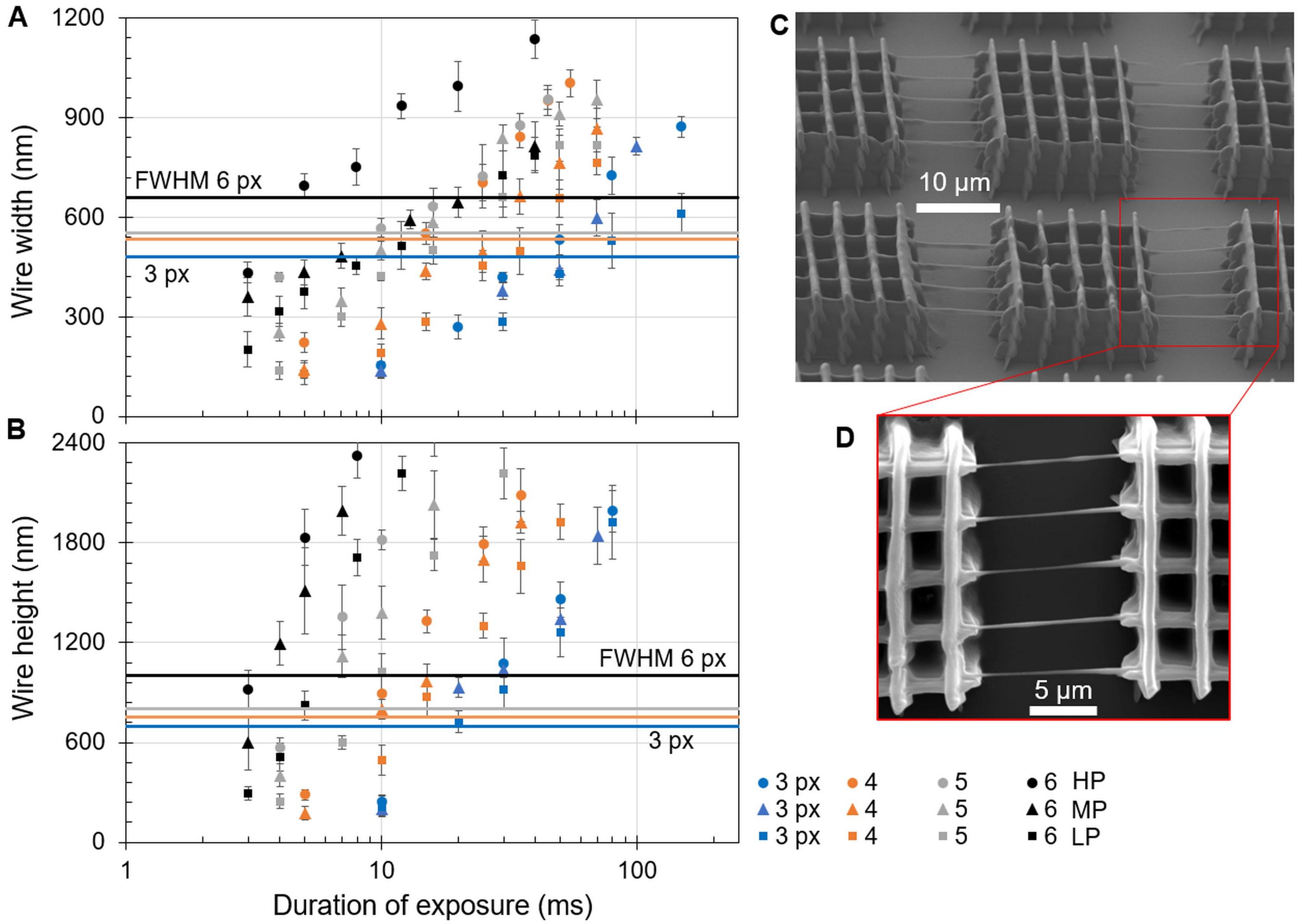
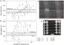
Fig. 2. Printed nanowires demonstrating nanoscale resolution of FP-TPL. (A) Width (along lateral direction) and (B) height (along axial direction) of suspended nanowires printed under different conditions. Width of lines in the projected DMD pattern was varied from 3 to 6 pixels with a fixed period of 30 pixels. Each pixel (px) maps to 151 nm in the projected image. Labels HP, MP, and LP refer to high (42 nW/px), medium (39 nW/px), and low (35 nW/px) power levels, respectively. All markers of a specific shape represent data points generated at the same power level, and all markers of a specific colour represent the same line width. Printing was performed with a femtosecond laser that had a center wavelength of 800 nm and a nominal pulse width of 35 fs and with a 60 × 1.25 numerical aperture objective lens. (C and D) Scanning electron microscope images of the suspended nanowire features.


